Catalan Institute of Nanoscience & Nanotechnology (ICN2)

Contact persons:

Elena Del Corro

The Catalan Institute of Nanoscience and Nanotechnology (ICN2)(www.ICN2.cat), created in 2003, is a research centre with currently about 200 people among researchers, technical support and administration. The research covers new material properties resulting from their nanometric scale; the development of methods for nanofabrication, growth, analysis, characterisation and manipulation of structures of nanometric dimension for nanoelectronics, spintronics, nanophotonics and nanophononics. ICN2 was awarded the coveted label of Excelencia Severo Ochoa by the Spanish Government, acknowledging its research excellence, the first in Spain in Nanoscience. The institute is the home of several ERC award holders and has an active technology transfer department.

Equipment / Facilities

Processing platform

Nanomaterials Growth Unit

The main purpose of the Unit is the deposition of thin nanostructured films by laser advanced techniques and the characterisation of structure and microstructure by advanced tools.

Nanofabrication Facility

The Nanofabrication Facility focuses on the design and development of nanofabrication methods and techniques for nanoscience and nanotechnology research and applications. The mission of the facility is to provide high quality services to both internal and external users.

Instrumentation Unit

The Instrumentation Unit focuses on the design, development, improvement and deployment of advanced state-of-the-art instruments for nanoscience and nanotechnology. The main aim is the creation of an integrated scientific and technical platform with a highly qualified multidisciplinary team capable of addressing challenging instrumental projects both for basic nanoscience research as well as for nanotechnology applications.

Biolab Facility

This new facility will provide the ICN2 researchers with a safe and reliable environment to advance in the application of nanotechnology to life sciences and medicine.

Mechanical Workshop Facility

The Facility offers a broad range of custom machining services for the design and fabrication of devices and components for the institute research.

Modelling platform

Characterization platform

Electron Microscopy Unit

The Electron Microscopy Unit focuses on the use of electron microscopy techniques for nanoscience and nanotechnology research and applications. The main aim is to provide scientific technical support to the ICN2 research lines and to neighbouring research centres, as well as developing and implementing novel related techniques. The laboratory has active collaborations with other research institutions and is becoming increasingly involved in European networks.

Photoemission Spectroscopy (XPS&UPS) Facility

ICN2 offers surface characterization by XPS and UPS to analyse the surface chemistry of a material in its unprocessed state or after treatment (fracturing, cutting or scraping in air or UHV to expose the bulk chemistry; ion beam etching to remove surface contamination; heating to study heat-induced changes; exposure to reactive gases or solutions, etc.).

X-Ray Diffraction Facility

X-Ray analysis is used for the study of the crystalline structure of solid materials, either in powder or in compact form, thin film or nanomaterials.

Molecular Spectroscopy and Optical Microscopy Facility

The molecular spectroscopy facility and optical microscopy is equipped with analytical instruments for performing both qualitative and quantitative analysis of chemical materials based on the interaction of electromagnetic radiation with matter.

SQUID Magnetometry Facility

The SQUID is a very sensitive magnetometer based on a superconducting quantum interference device. It integrates a detection system and a precision temperature control unit inside the bore of a high-field  superconducting magnet. Common uses of this equipment include field sweeps and hysteresis loops, moment vs. field and moment vs. temperature measurements and field and zero-field cool measurements.
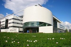
Expertise
Main Expertises
Beyond CMOS Neuromorphic Computing • Ferroelectric domain physics
• Ferroelectric domain wall physics
• Self-power electronics based on toxic-free 2D ferroelectric and ferroic materials (oxides, halide perovskites and MXenes)
Phonon engineering • Phonon transport in layered materials
• Nanoscale thermal transport physics and instrumentation
• Optomechanics
• Topological phononics
• Thermal properties of ferroelectrics and antiferroelectrics
• Electrocaloric effect
• Direct Spatially resolved Phonon detection by EELS-STEM
Small slope switches-NW/TFET/NEMS • Atomic scale STEM related characterization of the related heterostructure
• Nano-optoelectromechanical systems (NOEMS)
Alternative materials-2D layers • Ultrafast processes in graphene and related 2D materials
• Polycrystalline and amorphous 2D materials
• Free-standing oxide layers
• Domain Walls/oxide interfaces
• Thermal and elastic properties characterization
• 2D ferroelectric materials and MXEnes, Pb-free materials
Novel devices for ultra-low power • Spin, spin waves and heat interactions
• Computational nanoelectronics from ab initio
• Computational spintronics and electronics
• Self-power electronics based on 2D ferroelectric and ferroic materials (oxides, halide perovskites and MXenes)
1D • Atomic scale STEM related characterization of Nanowires and nanowire network systems
• Halide perovskites, Toxic-free halide perovskites, ferroelectric halideperovskties
Quantum Technologies & Very low temperature electronics • Rare-earth ions
• Quantum computation
• Atomic scale STEM related characterization of quantum systems
• Phonons impact on noise in quantum systems
More Moore Logic Nanodevices& circuits • Reconfigurable logics
• Electronic transport simulation using NEGF solvers.
• Simulation using self-consistent Schrödinger Poisson solvers
• Terahertz nonlinearities
• Atomic scale STEM related characterization
Memories • Magnetic random access memories
• Modeling for magnetic, ferroelectric, and multiferroic materials.
• Simulation of spin torque phenomena (STT-MRAM, SOT-MRAM)
• Ferroelectric memory devices
• Self-power electronics (transistors) based on 2D ferroelectric and ferroic materials (oxides, halide perovskites and MXenes)
Very low power devices • Phonon-electron and phonon-photon coupling in nano-optoemectronic devices
• Materials and devices for selff-power electronics (transistors, memoristors) based on 2D ferroelectric and ferroic materials (oxides, halide perovskites and MXenes)
High temperature electronics • Hot carriers in graphene and related 2D materials
More than Moore micro-nano-bio Sensors & Systems • DFT calculations of materials properties
• Chemical sensors simulations
• Graphene based electrodes and Graphene SGFET for biosensing
• Aptamer-based inkjet-printed flexible microfluidic devices
• Graphene-based electrochemical biosensors
Energy Harvesting • Spin caloritronics
• Thermoelecticity
• Ground state DFT calculations, and Molecular Dynamics
• Piezo electricity
• (Ultrafast) energy, charge and heat dynamics in condensed matter
• Bulk photovoltaic effect in ferroelectrics
• Piezoelectricity and Flexoelectricity
• Atomic scale STEM related characterization
• Photovoltaics, solution processable materials for printed perovskite solar cells.
• Integration of energy harvesters with photovoltaics ( solar, mechanical, vibrational energy, etc.)
RF devices & circuits • Spin torque induced ferromagnetic resonance
• Quantum control
• Coupling phonons to RF
• Terahertz spectroscopy and technologies
• NFC/RFID wireless biosensors and gas sensors
Photonics devices • Nanopatterning surfaces and metamaterial design for photonic components
• Photodetectors
• Nonlinear light converters
• Atomic scale STEM related characterization
• Radiative cooling surfaces
Power devices x
Flexible electronics • Electronic properties from first-principles
• Simulation of charge transport in organic matter (polaron transport)
• 2D spintronics
• Electronic properties from first-principles. Modeling different physical properties (structural, piezoelectric, magnetic, thermal, etc.)
• Graphene and 2D materials electronics
• Flexible graphene solution-gated field-effect transistors
• Flexible electronics based on 2D materials for interfacing with the nervous system; implantable medical devices
• Hydrophobic micro-nanostructured films
• Defectivity and dimensional metrology of nanopatterned devices
• Nanoparticles-based printed passive components
• Free-standing oxide films/membranes
• Thermal and electronic (experimental) transport in disordered (and crystalline) organic matter
• Stable organic glasses for optoelectronic and photovoltaic devices
• Solution processable materials (2D, halide perovskites, oxides) for printed electronics (lab scale and larger areas): inks and pastes
Smart systems& Systems design Smart systems • NFC wireless IoT sensors
Systems design x
Research interests
Research interests
Beyond CMOS Neuromorphic Computing • Ferroelectric domain physics for Neuromorphic computation
• Self-power, printed devices.
• Molecular electronics, ionic-electronic halide perovskites
• Defect engineering for the manipulation of conductance and retention (especially in ionic-electronic conductors)
Phonon engineering • Phonons as state variable
• Thermoelectric devices
• Frequency combs, synchronisation and chaos
• Topological phononic waveguides
• Thermal conductivity, thermal management and link to noise
• Strain control of electronic band structure in 2D materials
Small slope switches-NW/TFET/NEMS • 2D layers for 2DEG quantum systems
• Phonon-based devices in NOEMS based on phonon coupling to toher state variables
Alternative materials-2D layers • MXenes
• Graphene-integrated silicon photonics
• Ultrafast dynamics of energy, charge and heat
• Thermal conduction in 2D materials with periodic structures, defects and interfaces
• Defect engineering
• Vacancies and dipole formation
Novel devices for ultra-low power • Spintronics and new methods to study spin dynamics
• Molecular electronincs, nanointerfaces in low-dimensional systems and thermal properties
• Printed methods for device fabrication
1D • Graphene nanoribbons
• Nanowire networks
Quantum Technologies & Very low temperature electronics • Hybrid (semiconductor/superconductor) nanowire networks
• Superconducting qubits
• SiGe and III-V 2DEG systems
• Phononic crystals to control surface-noise in ion traps
More Moore Logic Nanodevices& circuits • 2-dimensional spintronics, including grapheme
• Spin devices.
• quantum logic devices
• MoS2 transistors architecture for elementary logic component
• Optical computing
• Terahertz for 6G
Memories • Unconventional ways of controlling the magnetization. Spin orbit torques (e.g. from spin-Hall effect)
• Understanding fundamental effects
Very low power devices • Coupled state variables
High temperature electronics • Hot-carrier photonics and (opto)electronics
More than Moore micro-nano-bio Sensors & Systems • Piezoelectrics, chemical sensors simulations
• Nanobiosensors and flexible lab-on-a-chip
• Nanobiosensors for healthcare and environmental fields applications
Energy Harvesting • Thermoelectric effects in ferromagnetic systems and heterostructures
• Thermoelectricity in topological insulators
• Spin thermoelectric effects
• Simulation of thermal transport in complex materials. Photovoltaics, multifunctional materials (flexoelectric, piezoelectrics, thermoelectrics, etc).
• Self powered neural stimulators
• Supercapacitors
• Thermal conductivity in Si membranes and phononic crystals and in other semiconductors, nanocomposites, organic-inorganic layers, etc.
• Nano-scale piezo electric devices for autonomous energy generation
• Perovskite solar cells
• Thermoelectrics
• Thermal rectification
• Nano-scale thermoelectric devices for zero-power devices
• Semiconductor based Solar cells (Si and new materials Zn3P2)
• Materials synthesis and ink fabrication
• Defect density manipulation
• Additive engineering
• Photovoltaic stability
• Self-powered devices
RF devices & circuits • Spin orbit torques
• Superconducting qubits
• Wireless sensors for neural sensing
• Phonon circuits
• Terahertz for 6G
• Modelling of antennas transmission
• IoT approach for big data generation
• Low-cost wireless sensors
Photonics devices • Active surfaces and metasurfaces
• Photodetection
• Nonlinear photonics
• Transceivers for data com
• Nanowire based single photon emitters and detectors.
• Thermal management of energy devices
Power devices x
Flexible electronics • PEDOT-PSS electrodes and PEDOT-PSS transistors for neural sensing
• Composite materials
• Simulation of charge transport in organic matter (polaron transport)
• Graphene, topological insulators and transition metal dichalcogenides
• Graphene and 2D materials electronics
• Wearable sensors
• MoS2 transistors architecture for flexible elementary logic component
• Roll-to-roll patterning of hierarchical structures
• Development of dimensional metrology for features < 20 nm • Inks and substrates for inkjet printing • Decoupling charge and thermal transport in organic materials through molecular orientation • Materials syntheses and ink fabrication • Printing methods for device fabrication • Flexible and stretchable technology based on 2D materials for neural interfaces; implantable devices for brain therapies
Smart systems& Systems design Smart systems • Modelling of antennas transmission
• IoT approach for big data generation
• Low-cost wireless sensors
Systems design x