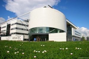
University of Twente
Contact persons:
Ray Hueting
University of Twente
Drienerlolaan 5
7522 NB Enschede
Netherlands
Processing platform
The University of Twente has a Nanolab facility comprising a 1200 m2 clean room for Nanotechnology experimentation with world class equipment.
Available equipment :
- Many tools including deposition tools (ALD, CVD and PLD), e-beam lithography, nanoimprint, implanter, sputter tools
- Many physical characterization tools including HRSEM, Dualbeam FIB, TEM, XRD, XPS, nanoprober, AFM, In situ spectroscopy in CVD/ALD
We are fully equipped for:
- Silicon process integration
- MEMS, microfluidics, silicon photonics
- Nanotechnology
Modelling platform
Silvaco, Synopsys, COMSOL
Characterization platform
- Wafer level DC and RF (up to ~100 GHz) electrical characterization
- Visible and infrared light emission characterization
- Chip level cryostatic characterization
| Main Expertises | ||
|---|---|---|
| Beyond CMOS | Neuromorphic Computing |
|
| Phonon engineering | x | |
| Small slope switches-NW/TFET/NEMS |
|
|
| Alternative materials-2D layers |
|
|
| Novel devices for ultra-low power |
|
|
| 1D | x | |
| Quantum Technologies & Very low temperature electronics |
|
|
| More Moore | Logic Nanodevices& circuits |
|
| Memories | x | |
| Very low power devices | x | |
| High temperature electronics | x | |
| More than Moore | micro-nano-bio Sensors & Systems |
|
| Energy Harvesting |
|
|
| RF devices & circuits |
|
|
| Photonics devices |
|
|
| Power devices |
|
|
| Flexible electronics |
|
|
| Smart systems& Systems design | Smart systems | x |
| Systems design | x |
| Research interests | ||
|---|---|---|
| Beyond CMOS | Neuromorphic Computing |
|
| Phonon engineering | x | |
| Small slope switches-NW/TFET/NEMS |
|
|
| Alternative materials-2D layers |
|
|
| Novel devices for ultra-low power |
|
|
| 1D | x | |
| Quantum Technologies & Very low temperature electronics |
|
|
| More Moore | Logic Nanodevices& circuits |
|
| Memories | x | |
| Very low power devices | x | |
| High temperature electronics | x | |
| More than Moore | micro-nano-bio Sensors & Systems |
|
| Energy Harvesting |
|
|
| RF devices & circuits |
|
|
| Photonics devices |
|
|
| Power devices |
|
|
| Flexible electronics | x | |
| Smart systems& Systems design | Smart systems | x |
| Systems design | x |


 Minatec – CROMA